
In recent years, the scientific research interest on nanomaterials has focused on the controlled growth of metal and semiconductor nanoparticles (NPs) and their multidisciplinary applications in very different fields, which range from nano-electronics to nano- photonics and nano-structured photovoltaic devices[1] [2] [3] or nanomaterials for pharmacology and medicine.
Metal and semiconductor nanoparticles have been grown by different chemical and physical methods including Physical Vapor Deposition, Chemical Reactions, and Laser Ablation Synthesis in Solution (LASiS). The last technique is the most used due its low cost and green chemistry characteristics[4]. However, many aspects of growth processes are still unknown and require more detailed studies.
In LASiS the NPs are obtained by irradiation of a pure metal or semiconductor with a pulsed laser (YAG or Kr-F). Laser and material parameters, such as bulk target, solvent and solutes, system temperature and pressure, laser wavelength, duration of irradiation strongly affect the shape and dimensions of the produced nanoparticles. The change of one or several of these parameters can result in the production of very different NPs in both sizes and dimensions. In this scenario, the ability to precisely control the characteristics of NPs by choosing appropriate laser and material parameters is strategic and requires a detailed understanding of the LASiS process4. When a laser beam impacts on a target surface a plume of ablated materials expands in the liquid solvent and the particles may nucleate and aggregate. There are many unclear points and open questions about the correlation between experimental conditions of LASiS, plume composition and size evolution of NPs. The answers for these questions are fundamental to better understand the growth process of nanoparticles and nanocrystals and to improve the engineering of nanoparticles production.
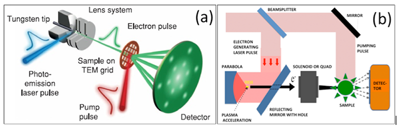
a) Sketch of a typical “conventional” Electron diffraction experiment; b) schematic setup for a laser-driven electron diffraction experiment
Several methods, involving many fields of material science (physics, chemistry, chemical engineering) have been developed to study nano-objects[5] (such as electron and X-ray diffraction, electron microscopy and atomic force microscopy). Among all structural methods Ultra Fast Electron and X-Ray Diffraction have a great potential for studying 4D structural dynamics, since the combination of high spatial resolution (on a sub-atomic scale, i.e. 8-10 picometers) and high temporal resolution (scale of chemical reactions i.e. sub 100 fs) makes it possible to perform online analysis of structural changes and energy redistribution[6]. The NP nucleation process (as specified in the following) occurs in a fs-ps temporal scale (depending on the pulse length of the laser irradiation). The greater challenge in the developing methods for LASiS control (with the aim of improving the engineering part and implementing industrial application of nanomaterials) is the probing of the structural dynamics. In order to resolve atomic-level details at the correct time resolution a stroboscopic probe, sensitive to atomic position, with a pulse duration of about 100 fs, must be used. The extremely short timescale allows only two options: short bunches of either electrons or X-rays must be used as a probe. With both sources, the challenge is twofold: generating femtosecond pulses, and producing sufficient flux to capture the structural details as close as possible to the single shot limit. Electrons and X-rays are equally capable of providing atomic level details of dynamics with high time resolution. However, the deposited energy and/or the elastic cross section for diffraction in different systems from X-ray or electron beam are very different, so that the choice of probe will depend strongly on the application[7]. The irradiation with X-rays can seriously damage the systems or influence the chemical reactions between atoms in particle nucleation. These problems can be solved using a low flux of X-rays. However, these are insufficient to reveal atomic details in a time scale of ps. The only X-ray sources with sufficient flux to fully resolve nano-structures are the third generation synchrotrons which provide a resolution time of about 100 ps or laser-based plasma X-ray sources with pulse duration of 100-200 fs, but relatively low X-ray flux[8]. Conventional accelerators generating 30 keV electrons have been able to achieve sub-picosecond electron pulses with sufficient flux to analyze complete structures in a few shots, without damaging or interferering with the analyzed sample[9]. The electron probes and the Ultra Fast Electron Diffraction (UED) are therefore the best choice to investigate the time and structural evolution of nanomaterials growth process.
The goal of this project is the generation of high-flux, high-energy laser-accelerated electrons with fs-scale temporal duration for performing Electron Diffraction experiments with improved electron parameters.
The project makes benefit of higher accelerating gradients (~TV/m), higher flux (~10^4 electrons per shot) and shorter pulse duration (25 fs at the source) that can be obtained with laser-plasma acceleration. Experiments are performed on different short-pulse laser facilities (e.g. our ALLS Laser and on the newly commissioned FORTH fs-laser (18 fs, 400 mJ, 10 Hz), manufactured by Amplitude). This project builds on preliminary and very promising experimental results related to this acceleration process that has already been achieved on the ALLS facility and published recently[10],[11],[12], achieving 23 keV electrons with 1.2 106 electrons per shot and tens of fs temporal duration. Besides testing “traditional” wakefield accelerated electrons, the project wants to explore a new acceleration regime, commonly called also “direct acceleration”, in which the polarization of the laser, used for the acceleration process, is modified with a specific waveplate. This allows having a strong longitudinal component on axis which allows boosting the acceleration process even further, and in particular for short pulse (
[1] Z. Ning, H. Tian, C. yuan, Y. Fu, H. Qin, L. Sun, H. Agren, Chem. Commun., 47, p. 1536, 2011
[2] A.M. Smith, S. Nie, Acc. Chem. Res., 43, p. 190, 2010
[3] A.P. Alivisatos, Nat. Mater., 2, p. 382, 2003
[4] V. Amendola, M. Meneghetti, J. phys. Chem. C, 113, p. 4277 (2009)
[5] A.S. Avilov, S.P. Gubin, M.A. Zaporozhets, Kristallografiya 58, 785 (2013)
[6] J. R. Dwyer et al.,, Philosophical transactions of the Royal Society A 364 (2006)
[7] R Srinivasan, V.A. Lobastov, C. Ruan, A. ZewailChim Acta 86 1763 (2003)
[8] S. Fourmaux, … V. Malka, A. Rousse and J. C. Kieffer Appl. Phys. Lett. 101 , 111106 (2012)
[9] B. Siwick, A.A. Green, C.T. Hebeisen, R.J. Miller, Chem. Phys. 299, 285 (2004)
[10] S. Payeur, S. Fourmaux, … F. Légaré, M. Piché, and J. C. Kieffer, Applied Physics Letters 101, 041105 (2012)
[11] S. Techert, F. Schotte,M. Wulff, Phys. Rev. Lett. 86, 2030 (2005)
[12] C. Varin, S. Payeur, … N. Thiré, T. Brabec, F. Legaré, J.C. Kieffer, M. Pichè, Applied Science 3, 70 (2013)